Combinatorial schemes
Elementary Boolean Functions
"NOT" (negation, inversion, NOT)
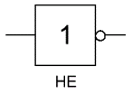 USSR designation of the NOT gate
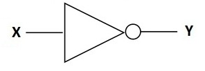 International designation of the NOT gate
 Truth table of the NOT gate
"NOT" In electronics a NOT gate is more commonly called an inverter. The circle on the symbol is called a bubble and is used in logic diagrams to indicate a logic negation between the external logic state and the internal logic state (1 to 0 or vice versa). On a circuit diagram it must be accompanied by a statement asserting that the positive logic convention or negative logic convention is being used (high voltage level = 1 or low voltage level = 1, respectively). The wedge is used in circuit diagrams to directly indicate an active-low (low voltage level = 1) input or output without requiring a uniform convention throughout the circuit diagram. This is called Direct Polarity Indication. See IEEE Std 91/91A and IEC 60617-12. Both the bubble and the wedge can be used on distinctive-shape and rectangular-shape symbols on circuit diagrams, depending on the logic convention used. On pure logic diagrams, only the bubble is meaningful.
"AND" (conjunction, logical multiplication)
 USSR designation of the AND gate
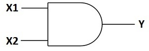 International designation of the AND gate
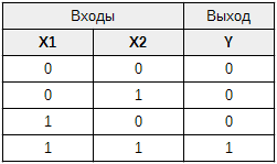 Truth table of the AND gate
gives a unit at the output only if a unit is supplied to all its inputs.
In other cases, it outputs zero. In logic circuits, the most common elements are And 2,
3, 4 inputs.
"OR" (disjunction, logical addition)
 USSR designation of the OR gate
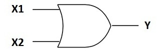 International designation of the OR gate
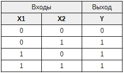 Truth table of the OR gate
"OR" gate returns a unit if at least one (or more) of its inputs is supplied with a unit.
Zero at the output appears only when zero is present at all inputs.
In logic circuits, OR elements without inversion are less common and generally have 2 or 3 inputs.
"NAND" (conjunction / logical multiplication with inverse)
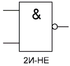 USSR designation of the NAND gate
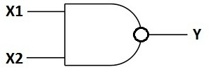 International designation of the NAND gate
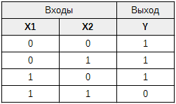 Truth table of the NAND gate
"NAND" gate outputs a signal opposite to the "AND" gate: if all inputs are fed
unit, the output is zero, in other cases, the output unit.
In logical microcircuits, NAND elements are used more often than others, typical microcircuits have from one to four
elements on 2, 3, 4 or 8 inputs.
"NOR" (disjunction, logical addition with inverse)
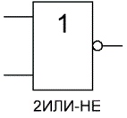 USSR designation of the NOR gate
 International designation of the NOR gate
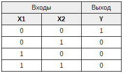 Truth table of the NOR gate
"NOR" gate outputs a signal opposite to the "OR" gate: gives zero in the case
if at least one (or more) of its inputs is supplied with a unit.
A unit at the output appears only when zero is present on all inputs.
In logic circuits, the most common elements are OR NOT at 2, 3, 4, and 5 inputs.
exclusive OR "XOR" (modulo 2 addition)
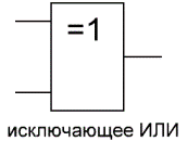 USSR designation of the XOR gate
 International designation of the XOR gate
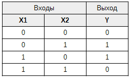 Truth table of the XOR gate
Элемент "XOR" (также называемый "неравнозначность") ‐ logic element
performing a logical addition operation modulo 2 on the input data, has two inputs and one output.
Often these elements are used in control circuits. A high voltage level will be output only if
when the input signals are not equal (on one unit, on another zero or on one zero, and on the other unit).
If the input contains two units or two zeros at the same time, the output will have zero ‐ this is in contrast to " OR ".
These logic elements are widely used in adders.
Combinatorial schemes
Combinatorial schemes are more complex devices that consist of logic gates and implement more complex logic functions.
Coder
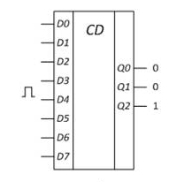 Truth table of the coder for 3 inputs and 8 outputs
An encoder converts the signal into a digital code, most often decimal numbers, into a binary number system.
The encoder has m inputs sequentially numbered with decimal numbers (0, 1, 2, ..., m - 1), and n outputs.
The number of inputs and outputs is determined by the dependence 2 n = m (see. Fig.). Symbol " CD " formed from the letters in the English word Coder.
Applying a signal to one of the inputs leads to the appearance on the outputs of an n-bit binary number corresponding to the input number.
For example, when applying a pulse to the 4th input, a digital code 100 appears at the outputs (Fig. 2, a).
Decoder
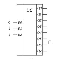 The symbol of the decoder for 3 inputs and 8 outputs
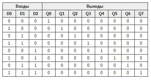 Truth table of the decoder for 3 inputs and 8 outputs
For the inverse conversion of binary numbers to small decimal numbers, decoders are used. The decoder inputs (see. Fig.) Are intended to supply binary numbers,
outputs are sequentially numbered with decimal numbers. When applying to the inputs of a binary number, a signal appears
at a specific output, the number of which corresponds to the input number. For example, when applying code 110, the signal will appear on the 6th output.
Multiplexer
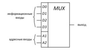 Условно-графическое обозначение мультиплексора на четыре входа
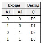 Таблица состояний мультиплексора на четыре входа
Multiplexer ‐ a device in which the output is connected to one of the inputs, in accordance with the address code.
Thus, the multiplexer is an electronic switch or commutator.
Demultiplexer
Demultiplexer schematically represents a decoder with permission input. Signal at one of the outputs
demultiplexer appears only when a signal is input to the permission input, in the absence of a permission signal,
there are no signals at all outputs. Thus, in fact, the signal is transmitted from the permission input to one
from exits.
In the produced logic circuits, as a rule, these functions are combined, and they are called decoders-demultiplexers.
There are so-called multi-channel switches ‐ these are schemes in which functions are combined multiplexer and demultiplexer. Such circuits have several inputs and several outputs, switching between which controlled by signals at the address inputs.
Adder and Half Adder
A single bit half adder is actually an "XOR" gate. The full single-digit adder, in addition to the "XOR" function output, has a carry output, the unit on which appears if there are units on both inputs.
ALU
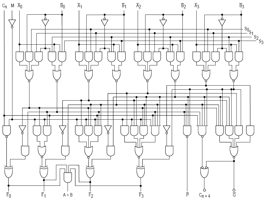 The 4-bit ALU combinational logic implemented in the TTL 24-pin chip model 74181, first developed and previously manufactured by Texas Instruments. Performs addition, subtraction, all elementary logic functions and bit shifts over two 4-bit operands. Does not contain registers
Arithmetic logic device is designed to perform operations on binary words received
at its entrances. ALU, which is a fully combinatorial (memoryless) device, has
inputs for two operands, inputs for selecting the operation to be performed on operands, output for output
the result of the operation, as well as additional carry outputs and flags.
The ALU block is part of the processor .
The classic ALU circuit was implemented in the 74181 chip.
Devices with memory
Triggers
Trigger is an electronic device that has two stable states and is capable of jump from one state to another under the influence of an external impulse.
Triggers, or rather trigger systems, call a large class of electronic devices with the ability to stay in one of two stable states for a long time and alternate them under the influence of external signals. Each trigger state is easily recognized by the value of the output voltage.
Each trigger state corresponds to a specific (high or low) output voltage level:
- the trigger is set to a single state - level "1" ;.
- trigger reset to zero - level "0" at the output.
The steady state is maintained for an arbitrarily long time and can be changed by an external impulse or shutdown supply voltage. T.O. a trigger is an elementary memory element capable of storing the smallest unit information (one bit) "0" or "1".
Triggers can be built on discrete elements, logic elements, on the integrated circuit or are part of the integrated circuit.
The main types of triggers include: RS- , D- , T- and JK- triggers. In addition, triggers are divided into asynchronous and synchronous. In asynchronous triggers, switching from one state to another is carried out directly with the arrival of a signal to the information input. In clocked triggers, in addition to information inputs, there is an input of clock pulses. Their switching is performed only in the presence of a resolving, clocking impulse.
RS-trigger
 Conditional graphic designation of the RS-trigger and pin assignment a) asynchronous, b) synchronous
RS-триггер has at least two inputs: S (set - set) - the trigger is set to a level state "1" and R (reset) - reset trigger to level state "0".
In the presence of input C, the trigger is synchronous - switching the trigger (changing the state of the output) can occur only at the moment of the arrival of a clock (synchronizing) pulse at input C.
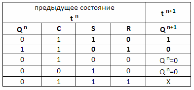 State table of synchronous RS-trigger
In addition to the direct output, the trigger can also have an inverse output, the signal at which will be the opposite.
Table 1 summarizes the states that a trigger can take during operation. The table shows the values
input signals S and R at some point in time t n and the state of the trigger (at the direct output) to the next
time t n + 1 after the arrival of the next pulses.
The previous state of Q n also affects the trigger's new state.
Thus if necessary, write to the trigger "1" - give a pulse to input S, if "0" - give a pulse to input R.
Combination of S = 1, R =1 is forbidden, because it is impossible to predict what state will be established at the output.
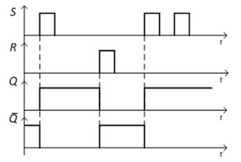 Timing diagrams of an asynchronous RS-trigger
The operation of a trigger can also be viewed using timing charts.
D-trigger
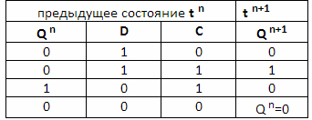 D-trigger status table
 D-trigger: a) graphic designation, b) timing diagrams of work
D-trigger (D means delay) has one information input and a clock (synchronizing) input.
D-flip-flop remembers and stores at the output Q the signal that was at the information input D at the time of arrival of the clock
pulse C.
Thus, the trigger stores the information recorded at C = 1.
T-trigger
 T-trigger: a) graphical designation, b) timing diagrams of work c) state table
T-triggers (T means tumble), also called countable triggers,
have one information input T. Each pulse (pulse drop) at the T-input (counting input) switches the trigger
in the opposite state.
JK-trigger
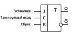 Условно-графическое обозначение JK-триггера
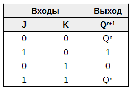 Сокращённая таблица состояний JK-триггера
JK-триггер (jump - kеер) has two information inputs J and K, and a clock input C.
The pin assignment of J and K is similar to the pin assignment of R and S, but the trigger does not have forbidden combinations.
If J = K = 1, he changes his state to the opposite.
With the appropriate connection of inputs, the trigger can perform the functions of RS-, D-, T-flip-flops, i.e. is a universal trigger.
Schmitt trigger
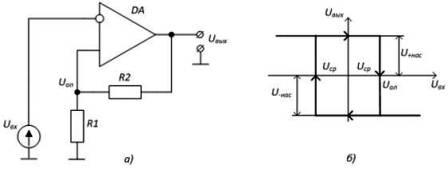 Schmitt trigger based on op-amp: a) the simplest circuit b) performance
Schmitt trigger ‐ is an comparator with positive feedback.
If the comparator is switching from "1" to "0" and vice versa occurs at the same voltage,
then the Schmitt trigger switches at different voltages. The reference voltage creates a positive feedback circuit R1R2, the input signal is supplied
to the inverting input of the op-amp. The figure shows the transfer characteristic of a Schmitt trigger.
With a negative voltage at the inventory input of the op-amp: U out = U + us .
This means that a positive voltage acts on the non-inverting input. With increasing input voltage at the moment
U in > Uninv. (U sw - switching) the comparator switches to the state U out = U -sat .
A negative voltage is applied to the non-inverting input. Accordingly, with a decrease in input voltage
at the time U in U uninv . (U sw ) the comparator switches to the state U out = U + sat .
Register
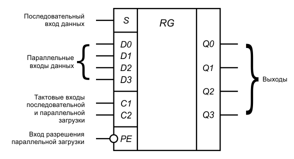 Conditional graphic designation and assignment of the findings of a four-bit parallel-serial register
Register - an electronic device designed for short-term storage and conversion of multi-bit binary numbers.
The register consists of triggers, the number of which determines how many bits of a binary number the register can store
& dash; bit width of the register. Logic elements can be used to organize triggers.
Registers are divided into parallel and serial by the method of input and output of information.
In a sequential register, triggers are connected in series, i.e., the outputs of the previous trigger transmit information
to the inputs of the subsequent. Clock inputs With triggers connected in parallel. Such a register has one information input.
and control input - clock input C.
In the parallel register, writing to triggers occurs simultaneously, for which there are four information inputs.
Counter
Counter , as well as register, is based on triggers. Applying a pulse to the counter input increases or decreases
binary code on its outputs. Many counters, when they reach the code limit, generate a carry signal to allow
increase their bit depth.
By the number of states, the counters are divided into binary, binary decimal, and programmable.
By organizing of internal communications, counters are asynchronous (based on the chain of JK triggers ,
included in the counting mode, i.e. with inputs J and K connected), synchronous with asynchronous transfer, and fully
synchronous (the fastest, but also the most complex type).